- 您现在的位置:买卖IC网 > Sheet目录1222 > ISL6144EVAL1 (Intersil)EVALUATION BOARD ISL6144 ORING
�� �
�
�ISL6144�
�P� loss� (� D1� )� =� P� loss� (� D2� )� =� ---------------� ?� V� F� =� 20A� ?� 0.5V� =� 10W�
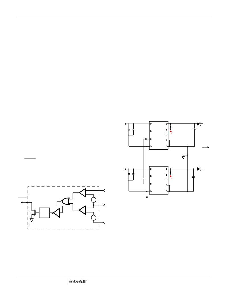
�D� 1�
�INPUT� BUS� 1�
�0.5V@� 20A�
�36VDC� TO� 75� VDC�
�CIN1� C� d1� 10�
�PC�
�220nF�
�100μF�
�-S�
�-IN�
�High� Voltage� Pass� and� Clamp�
�A� high� voltage� pass� and� clamping� circuit� prevents� the� high�
�output� voltage� from� damaging� the� comparators� in� case� of�
�quick� drop� in� V� IN� .� The� comparators� are� running� from� the� 5V�
�supply� between� HVREF� and� V� IN� .� These� devices� are� rated�
�for� 5V� and� will� be� damaged� if� V� OUT� is� allowed� to� be� present�
�(as� the� output� is� powered� from� other� parallel� supplies),� and�
�does� not� fall� when� V� IN� is� falling.� For� example,� if� V� IN� falls� to�
�30V,� V� OUT� remains� at� 48V� and� the� differential� Voltage�
�between� the� “-”� and� “+”� terminals� of� the� comparator� would� be�
�18V,� exceeding� the� rating� of� the� devices� and� causing�
�permanent� damage� to� the� IC.�
�Fault� Detection� Block�
�The� fault� detection� block� has� two� monitoring� circuits� (refer� to�
�Figure� 2):�
�1.� Gate� monitoring� detects� when� the� GATE� <� V� IN� +� 0.37V�
�2.� V� OUT� monitoring� detects� when� V� IN� -� 0.41V� >� V� OUT�
�These� two� outputs� are� ORed,� inverted,� level� shifted,� and�
�delayed� using� an� internal� filter� (� t� FLT� )�
�The� following� failures� can� be� detected� by� the� fault� detection�
�circuitry:�
�1.� ORing� FET� off� due� to� dead� short� in� the� sourcing� supply,�
�leading� to� V� IN� <� V� OUT�
�2.� Shorted� terminals� of� the� ORing� FET�
�3.� Blown� fuse� in� the� power� path� of� the� sourcing� supply�
�4.� Open� Gate� terminal�
�Application� Considerations�
�ORing� MOSFET� Selection�
�Using� an� ORing� MOSFET� instead� of� an� ORing� diode� results�
�in� increased� overall� power� system� efficiency� as� losses�
�across� the� ORing� elements� are� reduced.� The� use� of� ORing�
�MOSFETs� becomes� more� important� at� higher� current� levels,�
�as� power� loss� across� the� traditionally� used� ORing� diode� is�
�very� high.� The� high� power� dissipation� across� these� diodes�
�requires� special� thermal� design� precautions� such� as� heat�
�sinks� and� forced� airflow.�
�For� example,� in� a� 48V,� 40A� (1+1)� redundant� system� with�
�current� sharing,� using� a� Schottky� diode� as� the� ORing�
�(auctioneering)� device� (see� Figure� 3),� the� forward� voltage�
�drop� is� in� the� 0.4V� to� 0.7V� range.� Let� us� assume� it� is� 0.5V,�
�power� loss� across� each� diode� is� as� shown� in� Equation� 4:�
�I� OUT�
�(EQ.� 4)�
�Total� power� loss� across� the� two� ORing� diodes� is� 20W.�
�DC/DC�
�#1�
�+OUT1� =� 48V�
�+IN� +OUT�
�R� pb1�
�+S�
�C� cs1� SC� (Note� 11)�
�1nF� Figure� 14�
�PR�
�VOUT�
�(40A)�
�-OUT�
�+S�
�-S�
�5.� H� VREF� UV�
�The� FAULT� pin� is� not� latched� off� and� the� pull� down� will� shut�
�off� as� soon� as� the� fault� is� removed� and� the� pin� becomes� high�
�impedance.� Typically,� an� external� pull-up� resistor� is�
�connected� to� an� external� voltage� source� (for� example� 5V,�
�3.3V)� to� pull� the� pin� high,� an� LED� can� be� used� to� indicate� the�
�presence� of� a� fault.�
�GATE�
�INPUT� BUS� 2�
�36VDC� TO� 75� VDC�
�C� IN2� C� d2�
�100μF� 220nF�
�C� cs2�
�1nF�
�SECONDARY�
�GROUND�
�DC/DC�
�#2�
�+OUT2� =� 48V�
�+IN� +OUT�
�R� pb2�
�10�
�PC�
�SC� (Note� 11)�
�Figure� 14�
�PR�
�-IN�
�-OUT�
�D� 2�
�0.5V@� 20A�
�FAULT�
�DELAY�
�0.37V� +-�
�VIN�
�PRIMARY� GROUND�
�FIGURE� 3.� 1� +� 1� REDUNDANT� SYSTEM� WITH� DIODE� ORing�
�120μs�
�LEVEL� SHIFT�
�0.41V�
�+�
�-�
�VOUT�
�If� a� 5m� Ω� single� MOSFET� per� feed� is� used,� the� power� loss�
�across� each� MOSFET� is� as� shown� in� Equation� 5:�
�P� loss� (� M� 1� )� =� P� loss� (� M� 2� )� =� ?� ---------------� ?� ?� r� DS� (� ON� )�
�?� 2� ?�
�I� OUT� 2�
�(EQ.� 5)�
�P� loss� (� M� 1� )� =� (� 20A� )� ?� 5m� Ω� =� 2W�
�FIGURE� 2.� FAULT� DETECTION� BLOCK�
�8�
�2�
�Total� power� loss� across� the� two� ORing� MOSFETs� is� 4W.�
�In� case� of� failure� of� current� sharing� scheme,� or� failure� of�
�DC/DC� #1,� the� full� load� will� be� supplied� by� DC/DC� #2.� ORing�
�MOSFET� M2� or� ORing� Diode� D� 2� will� be� conducting� the� full�
�FN9131.7�
�October� 6,� 2011�
�发布紧急采购,3分钟左右您将得到回复。
相关PDF资料
ISL61853EVAL1Z
EVAL BOARD FOR ISL61853
ISL6227EVAL1
EVALUATION BOARD 1 ISL6227
ISL62386HIEVAL1Z
EVAL BOARD FOR ISL62386HI 32TQFN
ISL6291EVAL1
EVALUATION BOARD FOR ISL6291
ISL6292EVAL2
EVALUATION BOARD 2 ISL6292
ISL6296EVAL1
EVALUATION BOARD 1 ISL6296
ISL6298EVAL1
EVALUATION BOARD 1 ISL6298
ISL6298EVAL2
EVALUATION BOARD 2 ISL6298
相关代理商/技术参数
ISL6144EVAL1Z
功能描述:EVALUATION BOARD ISL6144 ORING RoHS:是 类别:编程器,开发系统 >> 评估演示板和套件 系列:- 标准包装:1 系列:PCI Express® (PCIe) 主要目的:接口,收发器,PCI Express 嵌入式:- 已用 IC / 零件:DS80PCI800 主要属性:- 次要属性:- 已供物品:板
ISL6144IR
功能描述:IC CTRLR MOSFET HV ORING 20-QFN RoHS:否 类别:集成电路 (IC) >> PMIC - O 圈控制器 系列:- 标准包装:1,000 系列:- 应用:电池备份,工业/汽车,大电流开关 FET 型:- 输出数:5 内部开关:是 延迟时间 - 开启:100ns 延迟时间 - 关闭:- 电源电压:3 V ~ 5.5 V 电流 - 电源:250µA 工作温度:0°C ~ 70°C 安装类型:表面贴装 封装/外壳:16-SOIC(0.154",3.90mm 宽) 供应商设备封装:16-SOIC N 包装:带卷 (TR)
ISL6144IR-T
功能描述:IC CTRLR MOSFET HV ORING 20-QFN RoHS:否 类别:集成电路 (IC) >> PMIC - O 圈控制器 系列:- 标准包装:1,000 系列:- 应用:电池备份,工业/汽车,大电流开关 FET 型:- 输出数:5 内部开关:是 延迟时间 - 开启:100ns 延迟时间 - 关闭:- 电源电压:3 V ~ 5.5 V 电流 - 电源:250µA 工作温度:0°C ~ 70°C 安装类型:表面贴装 封装/外壳:16-SOIC(0.154",3.90mm 宽) 供应商设备封装:16-SOIC N 包装:带卷 (TR)
ISL6144IRZA
功能描述:热插拔功率分布 W/ANNEAL 20LD 5X5 QF N ORING FET CONTRLR RoHS:否 制造商:Texas Instruments 产品:Controllers & Switches 电流限制: 电源电压-最大:7 V 电源电压-最小:- 0.3 V 工作温度范围: 功率耗散: 安装风格:SMD/SMT 封装 / 箱体:MSOP-8 封装:Tube
ISL6144IRZA-T
功能描述:IC CTRLR MOSFET HV ORING 20-QFN RoHS:是 类别:集成电路 (IC) >> PMIC - O 圈控制器 系列:- 标准包装:1,000 系列:- 应用:电池备份,工业/汽车,大电流开关 FET 型:- 输出数:5 内部开关:是 延迟时间 - 开启:100ns 延迟时间 - 关闭:- 电源电压:3 V ~ 5.5 V 电流 - 电源:250µA 工作温度:0°C ~ 70°C 安装类型:表面贴装 封装/外壳:16-SOIC(0.154",3.90mm 宽) 供应商设备封装:16-SOIC N 包装:带卷 (TR)
ISL6144IV
功能描述:IC CTRLR MOSFET ORING HV 16TSSOP RoHS:否 类别:集成电路 (IC) >> PMIC - O 圈控制器 系列:- 标准包装:1,000 系列:- 应用:电池备份,工业/汽车,大电流开关 FET 型:- 输出数:5 内部开关:是 延迟时间 - 开启:100ns 延迟时间 - 关闭:- 电源电压:3 V ~ 5.5 V 电流 - 电源:250µA 工作温度:0°C ~ 70°C 安装类型:表面贴装 封装/外壳:16-SOIC(0.154",3.90mm 宽) 供应商设备封装:16-SOIC N 包装:带卷 (TR)
ISL6144IV-T
功能描述:IC CTRLR MOSFET HV ORING 16TSSOP RoHS:否 类别:集成电路 (IC) >> PMIC - O 圈控制器 系列:- 标准包装:1,000 系列:- 应用:电池备份,工业/汽车,大电流开关 FET 型:- 输出数:5 内部开关:是 延迟时间 - 开启:100ns 延迟时间 - 关闭:- 电源电压:3 V ~ 5.5 V 电流 - 电源:250µA 工作温度:0°C ~ 70°C 安装类型:表面贴装 封装/外壳:16-SOIC(0.154",3.90mm 宽) 供应商设备封装:16-SOIC N 包装:带卷 (TR)
ISL6144IVZA
功能描述:IC CTRLR MOSFET ORING HV 16TSSOP RoHS:是 类别:集成电路 (IC) >> PMIC - O 圈控制器 系列:- 标准包装:1,000 系列:- 应用:电池备份,工业/汽车,大电流开关 FET 型:- 输出数:5 内部开关:是 延迟时间 - 开启:100ns 延迟时间 - 关闭:- 电源电压:3 V ~ 5.5 V 电流 - 电源:250µA 工作温度:0°C ~ 70°C 安装类型:表面贴装 封装/外壳:16-SOIC(0.154",3.90mm 宽) 供应商设备封装:16-SOIC N 包装:带卷 (TR)